Computer graphics, linux, and more from the cyberwitch's hut
Resuscitating an old fitness bracelet
A few years ago, I came across a mystery fitness bracelet. After a bit of research, it revealed itself to be a Xiaomi Mi Band 2. At the time, I didn't manage to get anything out of it, and in any case, the battery quickly ran out. Without the appropriate charger, I was left with a few dozen grams of e-waste-to-be…
That is, until march 2021 came around and I decided to do something about that black ring of rubber, plastic and glass that had been taking up space in my electronics salvage box.
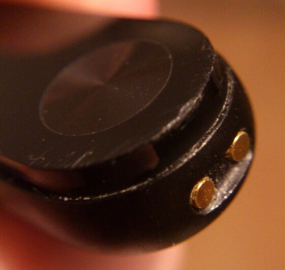
The actual active part of the Mi Band 2 is a small oblong and nearly featureless device, which is normally fitted inside a rubber bracelet while in use. This little device, as can be seen in the image below, only possesses two contacts, not even any kind of charging port.

In order to be able to recharge it, I'm left with two problems to be solved:
Presented with a mystery device that only possesses two electrical contacts, I took the liberty of assuming that I was dealing with some kind of USB charging, as with most modern gadgets. Which meant: 5V DC.
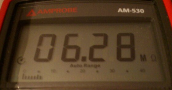
Once you run with this, the only thing left to figure out is the polarity. Based on an educated guess, it was probable that the charge circuitry contained a few diodes, which would translate to an asymmetry while measuring the resistance between the two poles. And lo and behold! I indeed measured an asymmetry: no continuity on one side, and a bit over 6 MΩ on the other, that last one being the polarity I needed to use!
So I'm looking at this small plastic thing, rounded all over, with no registering features (apart for maybe its screen), and I'm wondering how the heck will I be able to get any durable connection without resorting to soldering directly on the pads… And then it hit me: there is one place where the device is perfectly held: in its very own bracelet!
Going from there, it was just a matter of adding two contacts to the inside of the slot in the bracelet. For this purpose, I used the thinest wire I could get my hand on (a single strand from a multistrand copper wire) and threaded two pieces of it through the rubber of the bracelet using a sewing needle at the approximate position of the two contacts.
I then formed the inside ends in little spirals with my tweezers and added a bit of solder to try and get a larger contact area, and also prevent the wire from going all the way through.

To connect the tiny wires to the post connectors on the breadboard, instead of soldering I indulged in a bit of NASA-style wire wrapping (definitely didn't get anywhere close the acceptance standards).

Also, as can be seen on the above photo, I added some post terminals on the +5V side (here bridged by the jumper at the bottom), to be able to mesure the charging current with a multimeter.
While I was able to get the Mi Band 2 fully charged once using this setup, it is incredibly fiddly and fragile, requiring to spend a lot of time trying to blindly align the contacts, each time checking with the ohmmeter… It's tedious, to say the least.
Also having two wires permanently dangling from the bracelet doesn't make for the most ergonomic experience, to say the least.
All in all, good proof of concept, but definitely not production ready.
While the previous build validated my assumptions on the electrical side of things (nothing blew up, and the magic smoke is, to this day, still inside the device), it was time to step things up a notch on the mechanical design side of things.
Here are the few design goals I kept in mind for the second model:
The material study part of this project mostly consisted of me going "what do I have lying around that could work for this project?"
Quality engineering right there!
The options were mainly: cardboard (forget about the finished project ever looking good), wood (no good tools to work it at this small a scale), and finally a bit of scavenged large gauge magnet wire:

Combined with an old prototyping PCB to make a base, the magnet wire had some great potential, being at the same time pliable, strong (~1 mm diameter), and springy: a great material for this project.
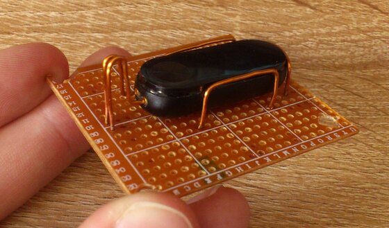
The assembly basically consisted of putting the device at the center of the PCB and eyeballing the placement of the three supports on the board. Then folding them to shape using a pair of pliers. And after that, given that the wire was enameled, sanding all the extremities that were to be soldered (burning the enamel away using a lighter works OK for headphone wire, but doesn't scale well here).
Then it was just a matter of soldering all the pieces in place, and bending the side supports just the right amount to act as clips holding the device in place.
As for the two wires on the left on the picture, they are the two contacts connecting with the device. I gave them a lot more length that would seem necessary, so that they would have some play to spring back and forth. That way, they can both apply some pressure on the contacts to guarantee a good electrical connection with the pads.
To bring power to this charger, what better way than the good old industry standard micro USB connector. After all, everyone, me included, has over the years accumulated quite the haul of USB power supplies and micro USB cables. Why not put one of those to good use here?
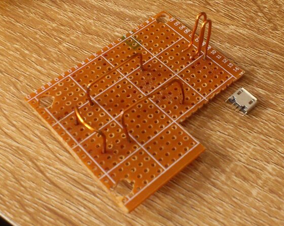
In terms of design, I fancied trying to break up the symmetrical silhouette with a recessed charging port. You'll see in the other pictures, I think it turned out great!

I used the same magnet wire as a support for the connector, to take the strain of plugging and unplugging the cable off of the power pins, that definitely aren't made to be load bearing. The wrap-around + solder design works very well to give a rock-solid connection between the magnet wire and the connector.

All in all, I'd call this a success, but were I to do it again, there are a few things I would have done differently. First I started soldering the supports like normal through-hole components, simply soldering to the pad around the hole. For structural components, that is a terrible idea: the supports are quite beefy and have enough leverage to strip off their pads. The solution would have been to keep a longer length of copper on the underside of the PCB and to solder it to multiple pads (like I did with the contacts and the USB connector support).
Also, the fit between the contacts isn't quite plug and play. It's close, but you still need to manually make sure both connectors end up on the device's contact pads. There is room for improvement there.
And finally, I didn't expect this project to look good at all, and seeing how it finally turned out surprisingly well, I'm kinda regretting not going full-on free form soldering, and getting rid of the PCB, just keeping the copper wire.
